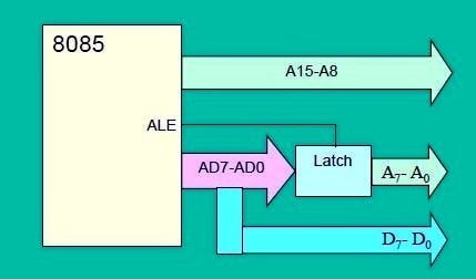
Demultiplexing Address/Data Bus AD7- AD0
Pin 30 of 8085 is the ALE pin
which stands for ‘Address Latch Enable’. ALE signal is used to demultiplex the
lower order address bus (AD0 – AD7). Pins 12 to 19 of 8085 are AD0 – AD7 which
is the multiplexed address-data bus. Multiplexing is done to reduce the number
of pins of 8085. Lower byte of address (A0 – A7) are available from AD0 – AD7
(pins 12 to 19) during T1 of machine cycle. But the lower byte of address (A0 –
A7), along with the upper byte A8 – A15 (pins 21 to 28) must be available
during T2 and rest of the machine cycle to access memory location or I/O ports.
Now ALE signal goes high at the beginning of T1 of each machine cycle and goes
low at the end of T1 and remains low during the rest of the machine cycle. This
high to low transition of ALE signal at the end of T1 is used to latch the
lower order address byte (A0 – A7) by the latch IC 74LS373, so that the lower
byte A0 – A7 is continued to be available till the end of the machine cycle.
The situation is explained in the following figure
Ø
From the above
description, it becomes obvious that the AD7–AD0 lines are serving a dual purpose
and that they need to be demultiplexed to get all the information.
Ø
The high order bits
of the address remain on the bus for three clock periods. However, the low
order bits remain for only one clock period and they would be lost if they are
not saved externally. Also, notice that the low order bits of the address disappear
when they are needed most.
Ø
To make sure we
have the entire address for the full three clock cycles, we will use an
external latch to save the value of AD7–AD0 when it is carrying the address
bits. We use the ALE signal to enable this latch.
Ø
Given that ALE operates as a pulse during T1, we
will be able to latch the address. Then when ALE goes low, the address is saved
and the AD7–AD0 lines can be used for their purpose as the bi-directional data
lines.
Ø
The high order address is placed on the address
bus and hold for 3 clk periods.
Ø
The low order address is lost after the first
clk period, this address needs to be hold however we need to use latch
Ø
The address AD7 –AD0 is connected as inputs to
the latch 74LS373.
Ø
The ALE signal is connected to the enable (G)
pin of the latch and the OC –Output control –of the latch is grounded
Data flow from memory to microprocessor unit (MPU)
Step1:- The
microprocessor places the 16-bit memory address from the pc on address bus.
Step 2 :- The
control unit send the control signal RD to enable the memory chip
Step3 :- The byte from
the memory location is placed on the data bus
Step 4 :- The byte is
placed in the instruction decoder of the microprocessor and the task is carried
out according to the instruction
REFERENCES
- R. S. Gaonkar, Microprocessor
Architecture, Programming, and Applications with the 8085, Fifth Edition,
Penram International Publishing (India) Private Limited.
- S Ghoshal, Microprocessor Based
System Design, Macmillan India Limited, 1996
- M. Mano, Digital Logic and
Computer Design, Prentice – Hall India
- B.
Ram - Fundamentals of Microprocessor and Microcontrollers
- “Microprocessors: Principles
and Applications” by A Pal
- “Microprocessors and
Microcontrollers : Architecture, Programming and Interfacing Using 8085,
8086 and 8051” by Soumitra Kumar Mandal
- “Introduction to
Microprocessors and Microcontrollers” by Crisp John Crisp
- “Microprocessors And
Microcontrollers” by A Nagoor Kani
- “Microprocessors And
Microcontrollers : Architecture, Programming and System Design 8085, 8086,
8051, 8096” by KRISHNA KANT
- “8 - Bit
Microprocessor”
by Vibhute


Comments
Post a Comment