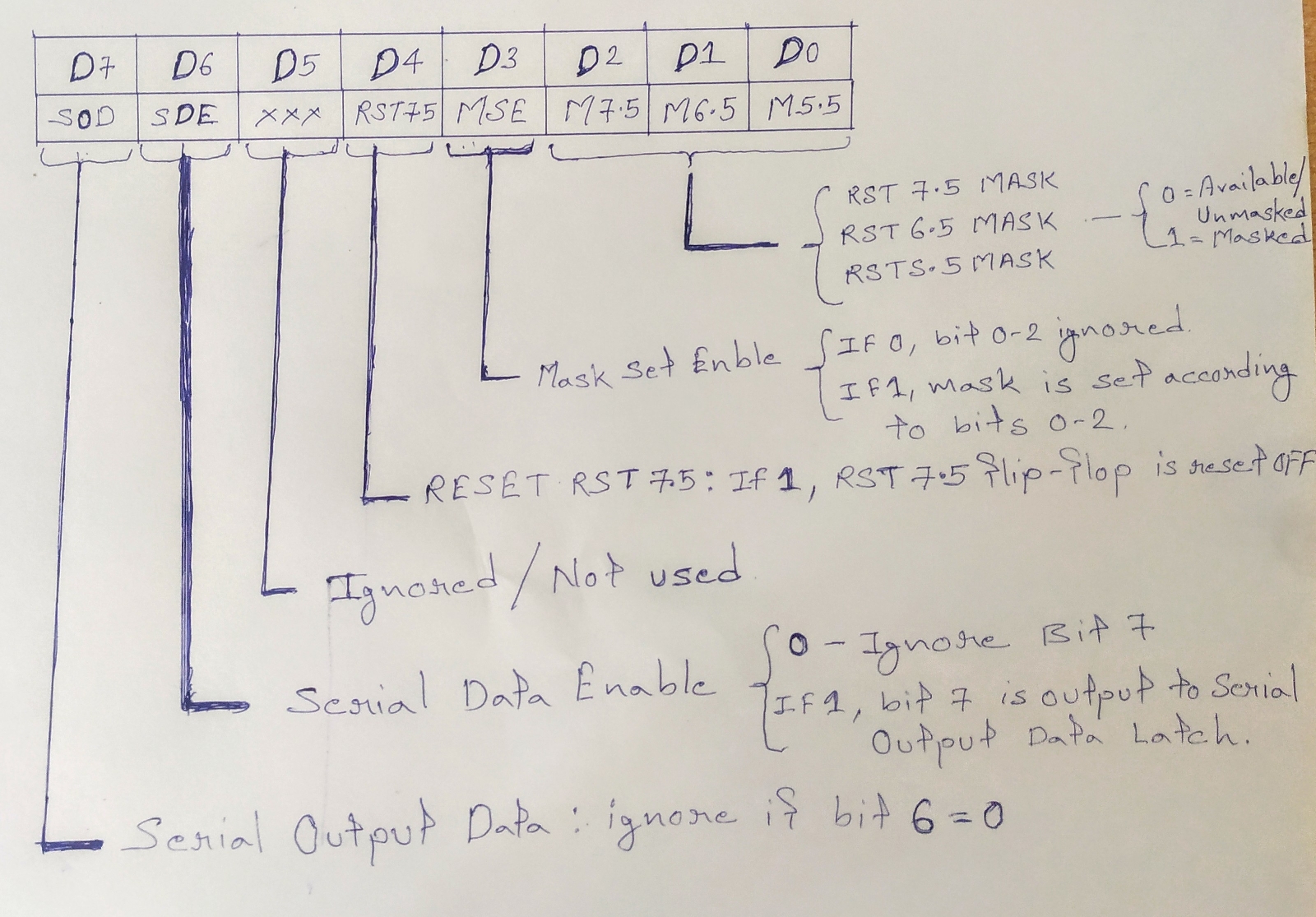
Pending Interrupts or Read Interrupt Mask (RIM) instruction
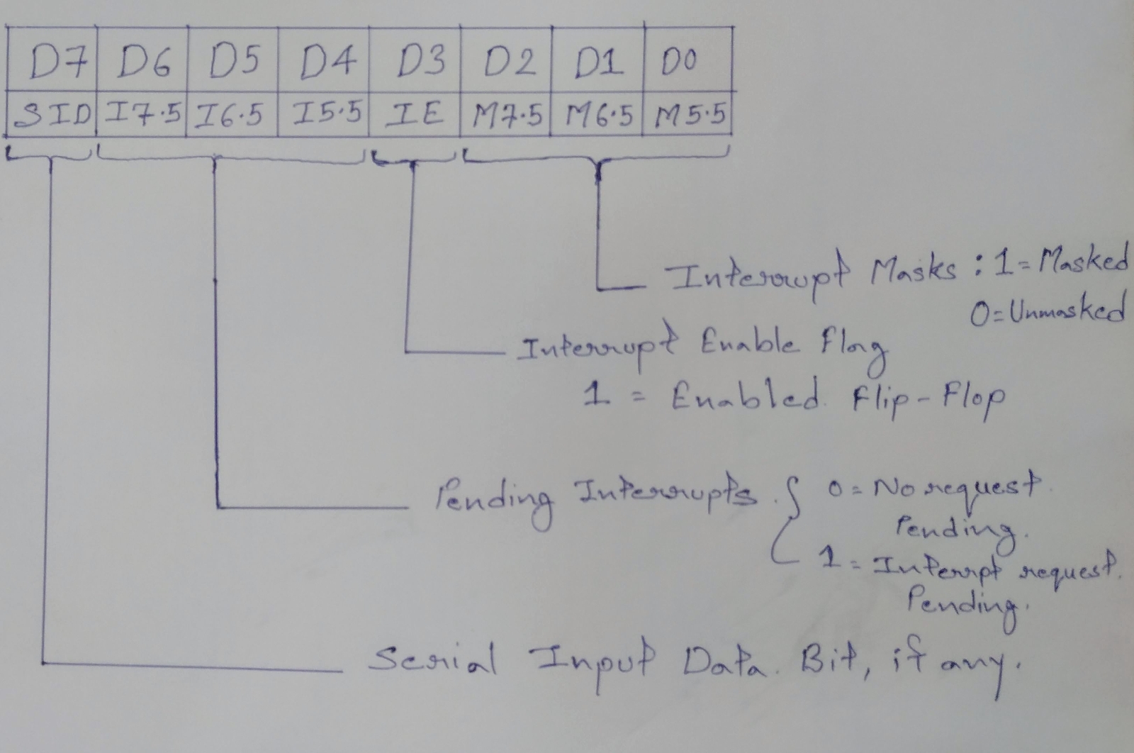
Pending Interrupts or Read Interrupt Mask (RIM) instruction Because there are several interrupt lines, when one interrupt request is being served other interrupt requests may occur and remain pending. The 8085 has an additional instruction called RIM (Read Interrupt Mask) to sense these pending interrupts. Read Interrupt Mask (RIM) – This instruction is used to read the status of the hardware interrupts (RST 7.5, RST 6.5, RST 5.5) by loading into the A register a byte which defines the condition of the mask bits for the interrupts. It also reads the condition of SID (Serial Input Data) bit on the microprocessor. Instruction RIM:- Read Interrupt Mask. The is a 1-byte instruction that can be used for the following functions. To read interrupt masks. This instruction loads the accumulator with 8 bits indicating the current status of the interrupt masks. To identify pending interrupts. Bits D4, D5 and D6 identify the pending interrupts. To receive seria...